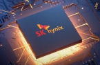
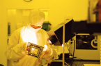
SK Hynix mass-produces 12-layer HBM3E for Q4 shipment
The latest HBM boasts the highest capacity among AI chips
By Sep 26, 2024 (Gmt+09:00)
When in S. Korea, it’s a ritual: Foreigners make stops at CU, GS25, 7-Eleven


Maybe Happy Ending: A robot love story that rewrote Broadway playbook
NPS yet to schedule external manager selection; PE firms’ fundraising woes deepen
Samsung steps up AR race with advanced microdisplay for smart glasses
Seoul appeal: Korean art captivates Indonesia’s affluent connoisseurs


SK Hynix Inc. said on Thursday it has begun mass-producing the world’s first 12-layer HBM3E with a capacity of 36 gigabytes (GB) for shipment later this year.
It did not identify the customers, but industry observers say they include Nvidia Corp., a graphics processing unit (GPU) major.
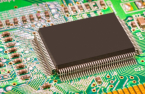
The latest version of high-bandwidth memory (HBM) vertically stacks 12 layers of 3 GB DRAMs. It compares with its predecessor 24 GB HBM3E, the maximum capacity of the fifth-generation HBM to date.
The 24 GB HBM3E interconnects eight 3 GB DRAM chips vertically. HBM chips are the best-performing DRAMs essential for AI applications, including large language models.
SK Hynix, the leader in the burgeoning HBM market, said its latest 12-layer HBM3E meets the world’s highest standards in all areas required for AI memory, including speed, capacity and stability. It has accelerated memory operations to 9.6 gigabits per second (Gbps), the highest memory speed for an HBM.
“SK Hynix has increased the capacity by 50% by stacking 12 layers of 3 GB DRAM chips at the same thickness as the previous eight-layer product,” it said in a statement. “To achieve this, the company made each DRAM chip 40% thinner than before and stacked vertically using TSV4 technology.”
TSV stands for through-silicon via and is an advanced packaging connection technology.
The company also solved structural issues that arise from stacking thinner chips higher by applying its mass reflow model underfill (MR-MUF) technology.
MR-MUF refers to the process of stacking semiconductor chips and features 10% higher heat dissipation performance compared with the fifth-generation HBM, or 24 GB HBM3E, according to SK Hynix.
SK Hynix is the world’s second-largest memory chipmaker after Samsung Electronics Co. But it is holding its lead in the HBM race.
In March, it became the industry’s first to mass-produce eight-layer HBM3E products with 24 GB for supply to Nvidia.
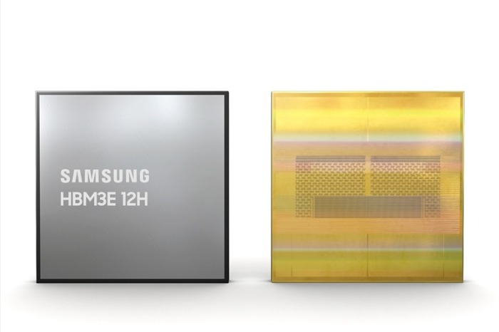
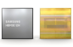
In comparison, Samsung delivered its eight-layer HBM3E samples to key customers in the second quarter of this year for qualification tests, said Kim Jae-june, executive vice president of its memory chip business, during a conference in July.
His remarks came about half a year after Samsung unveiled its 12-layer HBM3E with 36 GB.
Write to Eui-Myung Park at uimyung@hankyung.com
Yeonhee Kim edited this article.
-
 Korean chipmakersAnalysts rebut Morgan Stanley’s chip winter view; oversupply unlikely
Sep 22, 2024 (Gmt+09:00)
4 Min read -
 Korean chipmakersSK Hynix shares nosedive after Morgan Stanley downgrade
Sep 19, 2024 (Gmt+09:00)
4 Min read -
 Korean chipmakersSamsung Electronics, TSMC tie up for HBM4 AI chip development
Sep 05, 2024 (Gmt+09:00)
3 Min read -
 Korean chipmakersSamsung, SK Hynix up the ante on HBM to enjoy AI memory boom
Sep 04, 2024 (Gmt+09:00)
3 Min read -
-
 EarningsSK Hynix to supply 12-layer HBM3E to Nvidia in Q4; profit soars in Q2
Jul 25, 2024 (Gmt+09:00)
3 Min read -
 Korean chipmakersSamsung tipped to supply HBM3 to Nvidia for Chinese market
Jul 24, 2024 (Gmt+09:00)
2 Min read -
 Korean chipmakersSamsung to mass-produce HBM4 on 4 nm foundry process
Jul 15, 2024 (Gmt+09:00)
3 Min read -
 Korean chipmakersHBM chip war intensifies as SK Hynix hunts for Samsung talent
Jul 08, 2024 (Gmt+09:00)
4 Min read -
 Korean chipmakersSamsung launches dedicated HBM, advanced chip packaging teams
Jul 05, 2024 (Gmt+09:00)
3 Min read -
 Korean chipmakersSouth Korea sets sights on fostering EDA tech to win HBM chip war
Jun 28, 2024 (Gmt+09:00)
3 Min read -
 Korean chipmakersSamsung to launch 3D HBM chip packaging service in 2024
Jun 16, 2024 (Gmt+09:00)
2 Min read -
 Korean chipmakersSK Hynix works on next-generation HBM chip supply plans for 2025
May 30, 2024 (Gmt+09:00)
3 Min read -

-
 Executive reshufflesSamsung Electronics replaces chip head amid HBM crisis
May 21, 2024 (Gmt+09:00)
4 Min read -
 Korean chipmakersSamsung doubles down in HBM race with largest memory
Feb 27, 2024 (Gmt+09:00)
3 Min read