Korean chipmakers
Samsung to mass-produce HBM4 on 4 nm foundry process
Samsung to use its capability of chip design, production to maximize HBM4 performance; TSMC, SK Hynix to add 5 nm process
By Jul 15, 2024 (Gmt+09:00)
3
Min read
Most Read
S.Korea's LS Materials set to boost earnings ahead of IPO process


POSCO seeks restructuring for $1.9 bn injection in battery materials
Doosan Robotics to delist, wholly own cash-cow Doosan Bobcat
Korea to keep track of EV battery life cycles for recycling
Samsung to mass-produce HBM4 on 4 nm foundry process


Samsung Electronics Co., the worldŌĆÖs top memory chipmaker, plans to use its cutting-edge 4-nanometer (nm) foundry process for the mass production of a next-generation high-bandwidth memory (HBM) model, a core chip in powering artificial intelligence devices, to take on larger rivals in the sector ŌĆō SK Hynix Inc. and ┬ĀTaiwan Semiconductor Manufacturing Co. (TSMC).
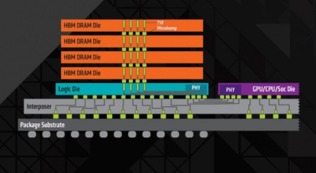
Samsung is set to utilize the 4nm foundry process for the logic die of the sixth-generation HBM4 chips, industry sources said on Monday. A logic die, which sits at the base of the stack of dies, is a core component of an HBM chip, which controls DRAM.
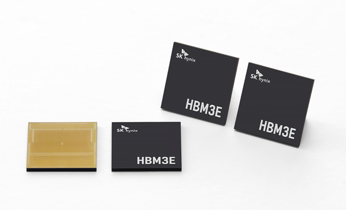
Memory chipmakers have manufactured logic dies for existing products such as HBM3E, but the sixth-generation model needs to go through foundry processes as it is equipped with customized functions required by clients.
The 4 nm node is SamsungŌĆÖs signature chip foundry manufacturing process with a yield of more than 70%. The company uses the process for the Exynos 2400 chipset, the brain of its flagship AI smartphone Galaxy S24 series.
ŌĆ£The 4 nm process is much costlier than the 7 nm and 8 nm but is significantly better than them in terms of chip performance and power consumption,ŌĆØ said an industry source. ŌĆ£Samsung, which manufactures HBM3E with the 10 nm process, aims to take the throne in the HBM sector by applying the 4nm process.ŌĆØ
The Suwon, South Korea-based tech giant had been expected to use the 7 m or 8 nm foundry process to produce HBM4 logic dies. Samsung has been operating the 7 nm process since 2019.
FIGHT AGAINST SK HYNIX, TSMC ALLIANCE
With the 4 nm process, Samsung is standing up to Hynix and TSMC, which have teamed up to strengthen their positions in the fast-growing AI chip market.
SK Hynix, the worldŌĆÖs top HBM supplier, joined hands with TSMC, the global foundry leader, for HBM4 in April as the South Korean company is focusing on the memory chip business. SK Hynix is the only supplier of the fourth-generation HBM3 chip to Nvidia, which controls over 80% of the market for graphics processing units, the core of AI computing tasks.
Samsung decided to deal with the partnership of the two NvidiaŌĆÖs major suppliers through its capabilities of designing and manufacturing foundry and HBM chips based on cooperation between its memory business and foundry division.
The 4 nm process, which has been applied since last year, requires sophisticated technology and double the resources of older processes. But it can manufacture high-performance and low-power chips.
Samsung aims to develop an HBM4 chip equipped with a high-performance logic die and beat competitors.
GROWING DEMAND FOR HIGH-PERFORMANCE, LOW-POWER CHIPS
Customers such as Nvidia and Advanced Micro Devices Inc. (AMD) have asked suppliers to develop HBM chips, which can quickly process large data with low power.
That came as AI accelerators, a high-performance parallel computation machine specifically designed to efficiently process AI workloads like neural networks, which consume a lot of electricity.
Samsung expects the 4 nm foundry process to facilitate the production of such HBM chips and prevail in the industry.
The company plans to seek optimization from the design stage of a logic die for maximizing the performance of HBM4 chips with its system LSI division, a fabless organization.
ŌĆ£Unlike TSMC and SK Hynix, it is our unique strength for chip designers to participate in HBM4 production,ŌĆØ said a Samsung executive.
The tech behemoth reportedly deployed staff of the system LSI division to the HBM development team recently established, according to industry sources.
SK Hynix and TSMC have taken measures to respond to SamsungŌĆÖs plan. The two companies have decided to add the 5 nm process to manufacture HBM4 logic dies in addition to the originally planned 12 nm process.
They also increased their talent base to improve the performance of HBM4 with SK Hynix hiring experienced logic design engineers.
Write to Jeong-Soo Hwang, Chae-Yeon Kim and Eui-Myung Park at hjs@hankyung.com
┬Ā
Jongwoo Cheon edited his article.
More to Read
-
 Korean chipmakersSamsung launches dedicated HBM, advanced chip packaging teams
Jul 05, 2024 (Gmt+09:00)
3 Min read -
 Korean chipmakersSK Hynix, TSMC tie up to stay ahead of Samsung for HBM supremacy
Apr 19, 2024 (Gmt+09:00)
4 Min read -
 ElectronicsSamsung Galaxy S24 heralds dawning of AI smartphone era
Jan 18, 2024 (Gmt+09:00)
3 Min read -
 Korean chipmakersSamsung Electronics to up AI chip foundry sales to 50% by 2028
Nov 20, 2023 (Gmt+09:00)
3 Min read -
 Korean chipmakersSamsung Elec to launch HBM4 in 2025 to win war in AI sector
Oct 10, 2023 (Gmt+09:00)
2 Min read -
 Korean chipmakersSamsung improves 4 nm foundry yields, on par with TSMC: analyst
Jul 11, 2023 (Gmt+09:00)
4 Min read
Comment 0
LOG IN