Korean chipmakers
Samsung to unveil 400-layer bonding vertical NAND for AI servers by 2026
A latecomer to the HBM and enterprise SSD segments, Samsung vows to strengthen its memory leadership with new technology
By Oct 28, 2024 (Gmt+09:00)
3
Min read
Most Read
When in S. Korea, it’s a ritual: Foreigners make stops at CU, GS25, 7-Eleven


Maybe Happy Ending: A robot love story that rewrote Broadway playbook
NPS yet to schedule external manager selection; PE firms’ fundraising woes deepen
Seoul appeal: Korean art captivates Indonesia’s affluent connoisseurs
K-pop stocks surge as China set to loosen cultural ban after 9 years


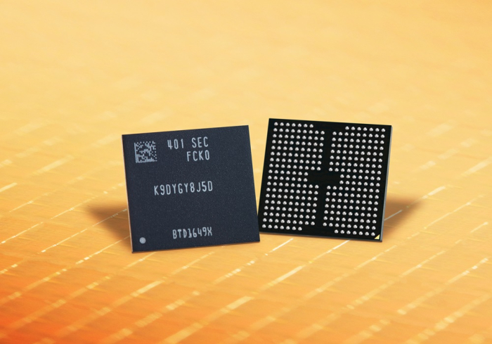
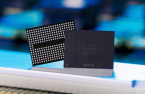
Samsung Electronics Co., the world’s largest memory chipmaker, plans to unveil a 400-layer vertical NAND flash chip by 2026 to lead the fast-growing storage device market amid the artificial intelligence boom.
According to the South Korean tech giant’s memory chip development road map obtained by The Korea Economic Daily, its Device Solutions (DS) division, which oversees its semiconductor business, aims to produce vertical NAND with at least 400 layers of cells vertically stacked to maximize capacity and performance as early as 2026.
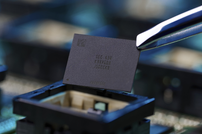
Samsung currently mass-produces 286-layer high-capacity V9 NAND flash chips.
In existing NAND chips, memory cells are stacked on top of the peripheral, which functions as the chip’s brain. However, stacking cells 300 layers and higher has often damaged the peripheral.
With the cutting-edge 10th-generation V NAND (V10), Samsung plans to apply an innovative bonding technology in which cells and the peripheral are created separately on different wafers and then bonded.
Samsung said this approach will enable "ultra-high" NAND stacks with large storage capacity and excellent heat dissipation, which is ideal for ultra-high-capacity solid-state drives (SSDs) used in AI data centers.
The chip, dubbed bonding vertical NANDFlash, or BV NAND, is a “dream NAND for AI,” according to the company.
In 2013, Samsung pioneered V NAND chips by launching vertically stacked storage cells — the first in the industry to do so — to maximize capacity.
According to Samsung, its BV NAND will increase bit density per unit area by 1.6 times.
Samsung aims to further develop its stacking technology by launching V11 NAND in 2027, boasting 50% faster data input and output speed.
The company also plans to introduce an SSD subscription service targeting tech companies looking to manage the high costs of AI semiconductor investments.
OVER 1,000-LAYER NAND CHIPS BY 2030
Samsung has vowed to solidify its leadership in the high-capacity, high-performance NAND flash market.
Competition is fierce for NAND-based storage devices because AI chips focus on inference, which requires large-capacity storage devices to store and process images and videos.
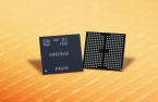
A NAND flash is a non-volatile memory chip that stores data even when the power is off. It is currently used in devices such as smartphones, USB drives and servers.
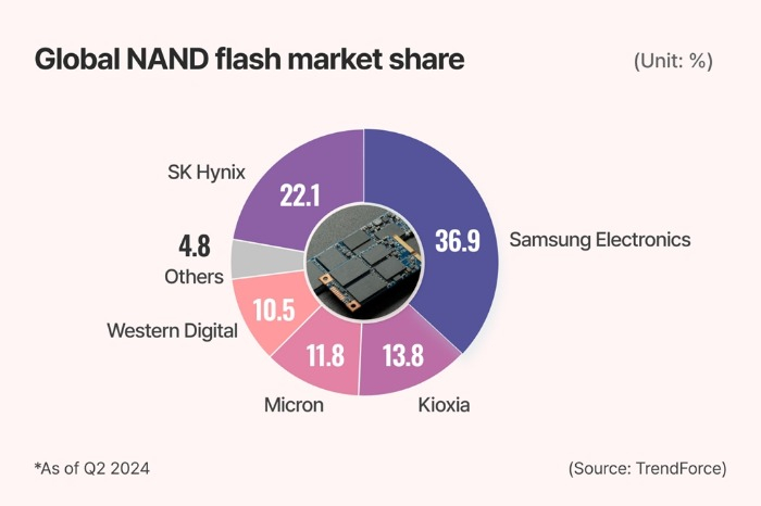
Samsung, already the dominant NAND player, controls 36.9% of the global market as of the second quarter, according to market tracker TrendForce.
Samsung executives said the company aims to develop over 1,000-layer NAND chips by 2030 for higher density and storage capabilities.
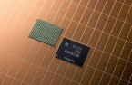
DRAM PROWESS
To strengthen its DRAM leadership, Samsung plans to release the sixth-generation 10-nanometer DRAM, or 1c DRAM, and seventh-generation 10 nm DRAM, or 1d DRAM, as early as the end of 2024 for use in advanced AI chips such as HBM4.
According to Samsung’s memory road map, it will unveil sub-10 nm DRAM, or 0a DRAM, in 2027.
The key feature of 0a DRAM is the application of the vertical channel transistor (VCT) 3D structure, similar to the technology used in NAND flash, to enhance performance and stability.
By vertically stacking cells, VCT DRAM can reduce interference between cells and increase capacity, according to Samsung.
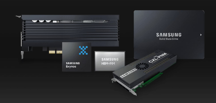
The company also plans to speed up the development of AI-specialized memory products beyond HBM, such as low power-processing in memory (LP-PIM).
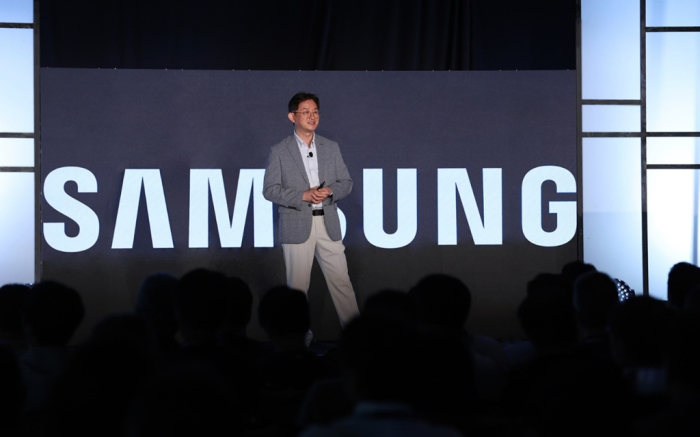
SAMSUNG CHIP HEAD JUN YOUNG-HYUN: A DETERMINED REFORMER
Samsung’s NAND push comes as Vice Chairman Jun Young-hyun, the head of the DS division, earlier this month flagged a drastic corporate revamp after the company posted worse-than-expected preliminary third-quarter earnings.
Despite its leadership in the overall DRAM market, Samsung is struggling in the HBM market to catch up to its crosstown rival SK Hynix Inc., the world’s No. 2 memory maker and the dominant supplier of high-end HBM chips to Nvidia Corp.
According to market research firm Gartner, the global memory market is expected to grow to $227 billion by 2026 from an estimated $92 billion in 2024.
Samsung expects the server DRAM and enterprise SSD (eSSD) markets to grow annually by 27% and 35%, respectively, between 2024 and 2029.
Write to Jeong-Soo Hwang, Eui-Myung Park and Chae-Yeon Kim at hjs@hankyung.com
In-Soo Nam edited this article.
More to Read
-
 Korean chipmakersSK Hynix chief says no delay in 12-layer HBM3E supply as demand soars
Oct 23, 2024 (Gmt+09:00)
3 Min read -
 EarningsSamsung chip head vows drastic revamp after flagging weak Q3 earnings
Oct 08, 2024 (Gmt+09:00)
4 Min read -
 Korean chipmakersArtificial intelligence creates DRAM divide between hot sellers, laggards
Oct 02, 2024 (Gmt+09:00)
3 Min read -
 Korean chipmakersSamsung mass-produces QLC V9 NAND to lead AI storage market
Sep 12, 2024 (Gmt+09:00)
3 Min read -
 Korean chipmakersSamsung Electronics, TSMC tie up for HBM4 AI chip development
Sep 05, 2024 (Gmt+09:00)
3 Min read -
 Korean chipmakersSamsung to unveil QLC-based NAND in H2 to lead AI storage market
May 22, 2024 (Gmt+09:00)
2 Min read -
 Korean chipmakersSamsung to produce 290-layer V9 NAND to win chip stacking war
Apr 11, 2024 (Gmt+09:00)
3 Min read -
 Korean chipmakersSamsung flexes NAND muscle with high-capacity microSD cards
Feb 28, 2024 (Gmt+09:00)
3 Min read
Comment 0
LOG IN