Korean chipmakers
Samsung, AMD to collaborate on 3 nm GAA tech chipmaking
Leveraging its closer ties with AMD, Samsung aims to overtake its bigger foundry rival TSMC
By May 29, 2024 (Gmt+09:00)
2
Min read
Most Read
Samsung steps up AR race with advanced microdisplay for smart glasses


When in S. Korea, it’s a ritual: Foreigners make stops at CU, GS25, 7-Eleven
Maybe Happy Ending: A robot love story that rewrote Broadway playbook
NPS yet to schedule external manager selection; PE firms’ fundraising woes deepen
US auto parts tariffs take effect; Korea avoids heavy hit


Samsung Electronics Co., the world’s largest memory chipmaker, is expected to expand its partnership with US-based fabless semiconductor designer Advanced Micro Devices Inc. (AMD) into cutting-edge 3-nanometer chip processing technology.
For years, the two companies have collaborated on developing the graphics processing unit (GPU) for smartphones and high-bandwidth memory (HBM) chips, which recently emerged as the red-hot DRAM for artificial intelligence devices.
If the two partners team up on the 3 nm node technology, it will help Samsung, the South Korean tech giant, narrow its market-share gap in foundry, or contract chipmaking, with market leader Taiwan Semiconductor Manufacturing Co. (TSMC), analysts said.
AMD Chief Executive Lisa Su, who attended Imec’s ITF World 2024 conference in Belgium, unveiled the company's plan to mass-produce next-generation chips using 3 nm Gate-All-Around (GAA) technology at the forum.
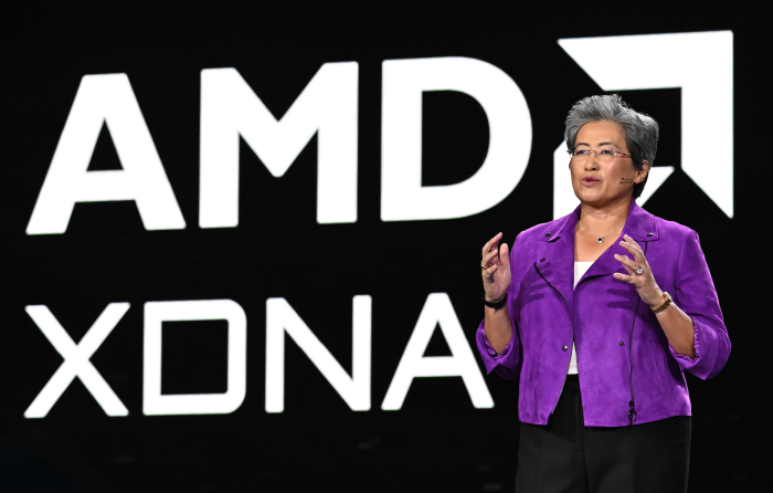
She touted 3nm GAA transistors as the catalyst to improving efficiency and performance, along with improvements in packaging and interconnects, resulting in more cost-effective, power-efficient AMD products.
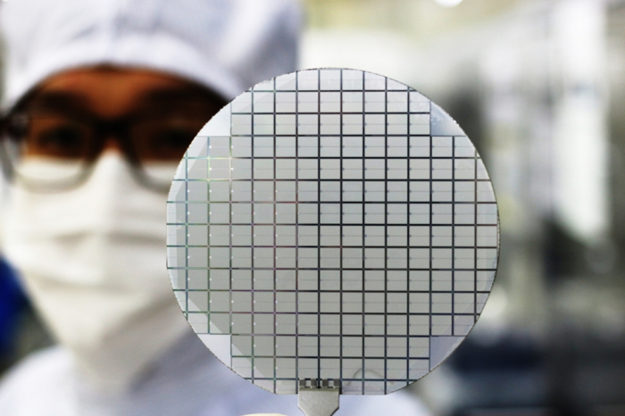
Samsung is currently the only chipmaker to commercialize GAA-based 3 nm chip processing technology.
Last year, Samsung, in a global first, applied a 3 nm process node to the manufacture of advanced chips based on GAA transistor architecture.
“Lisa Su’s comments are viewed as effectively formalizing AMD’s 3 nm foundry collaboration with Samsung,” said an industry official.
Sources said AMD is closing ranks with Samsung as TSMC’s 3 nm technology is fully booked for its clients such as Apple Inc. and Qualcomm Inc.
WIDENING SAMSUNG-AMD PARTNERSHIP
AMD, which specializes in developing central processing units (CPU) for servers, is expanding its business in AI accelerators, which use machine learning technology to process large amounts of data.
Last year, the two companies signed a multi-year partnership extension agreement to bring the US chip designer’s multiple generations of high-performance, ultra-low-power Radeon graphics functions to an expanded portfolio of Samsung’s Exynos application processors.
Samsung also agreed to provide HBM chips and turnkey packaging services to AMD as part of a broader partnership.
The GAA architecture, a next-generation foundry microfabrication process, is a key technology that improves electrostatic properties, which translate into increased performance, reduced power and optimal chip designs.
Samsung said the 3 nm GAA technology offers a 30% performance boost, a 50% reduction in energy consumption and a 45% decrease in chip area compared with the previous processing node.
Samsung aims to mass-produce 2 nm chips based on GAA architecture starting in 2025.
TSMC and other foundry companies mainly use a technology called the fin field-effect transistor (FinFET) process. It is also called the fin transistor because its structure resembles a fish’s dorsal fin.
TSMC, the foundry market leader, reportedly plans to apply GAA technology to its chip manufacturing process from the 2 nm node.
Samsung is the world’s largest memory chipmaker but a distant runner-up to TSMC in the foundry segment in terms of market share.
Write to Jeong-Soo Hwang at hjs@hankyung.com
In-Soo Nam edited this article.
More to Read
-
 Korean chipmakersSamsung set to supply HBM3, packaging services to AMD
Aug 22, 2023 (Gmt+09:00)
1 Min read -
 Korean chipmakersSamsung, AMD extend partnership for next-generation graphic chips
Apr 06, 2023 (Gmt+09:00)
3 Min read -
 Korean chipmakersSamsung unveils industry’s first 12 nm DRAM, compatible with AMD
Dec 21, 2022 (Gmt+09:00)
2 Min read -
 Korean chipmakersSamsung sets sights on GAA tech to overtake TSMC in foundry
Nov 29, 2022 (Gmt+09:00)
6 Min read -
 Korean chipmakersSamsung to make 2-nanometer GAA chips by 2025 to overtake TSMC
Oct 07, 2021 (Gmt+09:00)
3 Min read
Comment 0
LOG IN